The master of us all
Practically everything electrical we care to determine from an atom--and a lot of others things about that atom for that matter--can be observed from its concentration of valence electrons. One of the more immediate physical consequences is the structure of an element or a compound; how the bond angles and the covalent pair locations affect the physical positioning of atoms within a structure. The most popular semiconductor device elements--silicon and germanium--have four valence electrons, and tend to form highly ordered crystal structures with themselves and four other neighbors. When silicon atoms bond with other silicon atoms, they tend to form a diamond lattice. At this point however, since each of the four valence electrons of the silicon atom is bonded with another valence electron, there are no free electrons in the volume of the structure, except perhaps at the edges. Thus, pure silicon is not really a semiconductor. In fact, were it not for thermal processes freeing electrons from their covalent bonds, silicon would be a very good insulator.
Left to its own devices at room temperature, a structure of pure silicon will only occasionally have enough thermal energy to knock an electron out of the valence band into the conduction band, where it floats around. This action leaves a bond of one electron in the lattice and a positively charged ion of silicon; this missing bond is called a "hole" which a roaming electron will come and fill. For any given temperature at any given time, there are a given number of electrons and holes in the silicon lattice; since these carry either a positive or a negative charge, they are referred to as "charge carriers." The amount of charge carriers per cubic centimeter in a pure silicon lattice is called the "intrinsic carrier concentration" and is given by
ni = BT3/2e[-Eg/2kT]
Where T is the temperature in Kelvin, e is the charge of an electron, Eg is the material's bandgap energy, k is the Boltzmann constant, and B is an experimentally determined material-specific coefficient.
At room temperature, silicon has an intrisic carrier concentration of 1.5 * 1010 electrons per cubic centimeter. This is not a lot of electrons (it's about 2.4 nanocoloumbs of charge), especially when one learns that there are about 5.0 * 1022 atoms of silicon in a cubic centimeter of pure silicon. The magic happens when we add impurities to the silicon lattice.
"Impurites" in the lattice are simply atoms which are not silicon. Specifically, the silicon is "doped"--injected with atoms--with Group III materials (the most common is boron) and Group IV materials (the most common is phosphorous). Like all Group III elements, boron has three valence electrons; when it bonds with four neighboring silicon atoms, it gains an extra electron in its valence shell and becomes a negative ion. Similarly, phosphorous (like all Group IV elements) has five valence electrons and when it bonds with silicon there is one left-over electron not in a covalent bond; when this electron is loosed from the phosphorous atom, the atom is positively charged. The phosphorous is a "donor impurity" because it donates an electron; since there are many more electrons than holes in the phosphorous region, the electron is the "majority charge carrier" in the phosphorous doped silicon, which is now called "n-type material" (the "n" being "negative" charge). Similarly, the boron is an "acceptor impurity" because the boron atom accepts electrons; the boron-doped silicon is called "p-type material" and the holes are the majority charge carrier in the material. The doping of the silicon greatly increases the amount of charge carriers in the material, and the material's "extrinsic carrier concentration" is given by
nopo = ni2
Where no is the number of electrons, po is the number of holes, and ni is the intrinsic carrier concentration. For example, whereas before we had 1.50 * 1010 carriers, we now have 2.25 * 1020, which is a dramatic increase.
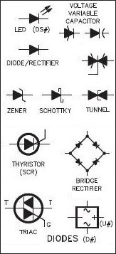
Diode
With the premilinary chemistry and jargon covered, we can now get into the physics. Let's slap together a piece of n-type material and p-type material and observe what happens (Actually, the n-type and p-type materials are created from one piece of silicon so they're already together).
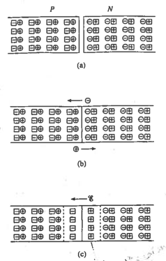
Before the joining, both the n-type and p-type material are electrically neutral. At the joining, the "holes" in the p-type material diffuse into the n-type material (leaving behind negatively-charged acceptor atoms); and likewise, the electrons in the n-type material diffuse into the p-type material, leaving behind positively-charged donor atoms. Two important things happen. First, the electric neutrality of the type materials are upset near the joining of the materials as they lose their balancing holes and electrons; the charge differences between the donor and acceptor atoms creates an electric field and thus a potential difference, and since the atoms are fixed, that field is maintained. The positive charge end repels the further diffusion of holes and the negative charge end repels the further diffusion of electrons. Second, the holes are filled by the electrons; since holes/electrons exist as a charge carrier pair, the charge carrier disappears. Thus, in the center near the joining, there are barely any charge carriers; this region of the p-n junction (as it's called) is called the depletion region. The picture shows a simplification of the diffusion action.
This electric field prevents the further movement of charge carriers as long as it is maintained. If an EMF source is connected with the positive potential at the n-type (i.e. the field from the source is in the same direction as the field from the p-n junction, called the "built-in voltage") the electric field increases and further pushes back the holes and the electrons, increasing the width of the depletion region. This condition is called "reverse bias." Eventually, if the external voltage is large enough (typical values are 90 V - 100 V) the depletion region will span the entire length of the p-n junction and the whole junction become electrically neutral, allowing current to flow. This condition is called "reverse breakdown." If the EMF source is connected the opposite way--positive potential at the p-type terminal, called "forward bias"--the built-in electric field decreases in strength due to superposition. Once the internal junction field is sufficiently weak, it can no longer prevent current flow and the holes move through the n-type material and the electrons move through the p-type material. For silicon, the required voltage for this to occur is about 0.6 V - 0.7 V. This behavior at the p-n junction--current designed to flow one way but not the other--effectively creates a diode, replacing tube-element diodes due to their smaller size, power dissipation, and reliability.
Transistor
If you went back in time to a little over a century ago, you would find no such thing as "electrical engineering." Electricity was largely considered to be the domain of physicists and course studies in electrical engineering were not be offered at any university in the world until the late 1880s. Up until that point, physicists put electricity to work in communication systems such as telegraphs and radios using the power of vacuum-tube circuit elements. In addition, prior to the 1940s or so, "electrical engineering" as a specialty meant delving deeper into using electricity as energy, powering homes, businesses, and machines. Then, everything changed.
The story of the transistor differs depending on who you ask. The main story is that in 1947, two American engineers at AT&T--Walter Brattain and John Bardeen--were conducting experiments with metal and a piece of germanium. If a pair of gold-plated contacts touched a piece of germanium, the signal running through the contacts would be reproduced across the germanium with more power. A third Bell Labs engineer, head of Solid State Physics Group William Shockley, recognized the signal amplification potential of this setup (amplification was used long before the transistor, in the days of the vacuum tube element) and went to work greatly refining and documenting the transistor. About a month later, in December, the trio had created the first semiconductor point-contact transistor.
The point-contact transistor worked, but the design as the trio conceived it was highly unreliable and that's why it has not survived into the present day. After legal issues and group consternation over patent issues and who should be named and awarded for what, William Shockley--who was largely responsible for the research into the point-contact transistor--went to develop further his own, superior transistor design after not having his name and effort recognized in the "Bardeen-Brattain point contact design" patent. The reason for this is because Shockley's design seemed too similar to a patent filed in the late 1920s by Austro-Hungarian physicist Julius Lilienfeld (his patent had no working designs and no further research attached to it so he was otherwise largely shafted and ignored).
Lilienfeld had thought of the idea of a "Field-Effect transistor" (the FET, pictured as the top diagram in the image above); an external electric field from some EMF source between the gate and source terminals would penetrate into the semiconductor, altering its conductivity and creating a conductivity channel between the n-type materials of the gate and drain terminals, allowing for current flow between those terminals controlled by an external electric field. William Shockley had created the bipolar junction transistor (BJT), which works by injecting electrons into the emitter terminal and applying an electric field across the emitter and collector terminals. Then, electrons are injected through the base terminal (the base p-type material is heavily doped), creating an "excess minority carrier distribution" (the electrons are called minority carriers because there are less of them in the p-type material than there are holes) near the emitter terminal; the charge distribution in the base creates an electric field which allows the emitter electrons to shoot across the base p-type without electron/hole recombination and a loss of electrons. Along with his transistor, Shockley also developed several semiconductor equations to describe the current flow relative to the control voltage of the p-n element. One equation, the Shockley diode equation, relates the current through a diode to the voltage across the diode. The equation is
I = IS[eVD/(nVT) - 1]
Where IS is the reverse bias scale current, VD is the voltage across the diode, VT is the thermal voltage determined by equation
VT = kT/qAnd n is the "ideality factor," a manufacturing-specific value from 1 to 2 where a value of 1 marks a completely ideal diode.
Similar equations exist for the FET and the BJT transistor (notice that the BJT equation is pretty much the exact same):
I = K[2(vgs - Vto)vDS - v2DS] [FET] and iE = IES[eVBE/(VT) - 1] [BJT]For the FET, K is a contstant depending on the geometry of the metal gate plate used to induce voltage in the FET, vGS is the voltage across the gate and source terminals, Vto is the "turn-on voltage" (the amount of voltage needed to allow current to flow in the forward-bias configuration) and vDS is the voltage across the drain and source terminals.
For the BJT, IES is the same as IS in the diode equation, VBE is the voltage across the base and emitter terminals, and, VT is also the thermal voltage.
The BJT and the FET, due to their ease of manufacturing and reliablity, have become the dominant types of transistors today (the FET is the transistor most used in microprocessor and other computer circuits).
As you can tell, the transistor has been a huge hit with civilization. Its signal amplification and switching applications were great enough. But then there were two more concurrent developments along with the transistor that were to irreversably change the course of human civilization. In 1937, electrical engineer Claude Shannon presented his master's thesis A Symbolic Analysis of Relay and Switching Circuits which showed how electrical switching elements could be used to implement Boolean logic (first implemented using vacuum-tube switches and then with transistors). Later, in 1958, Jack Kilby and a team of engineers at Texas Instruments toyed with the idea of the integrated circuit; a slab of semiconductor material that could be machine-etched and altered to perform all the functions a big bulky circuit could--resistors, capacitors, etc. With the theoretical mathematical basis laid out along with the means to implement it effectively and cheaply (transistors and integrated circuits) engineers got to work and the rest is history.