Semiconductors
Most of our modern electronic
technology is centered around semiconductors. From transistors
and diodes to integrated circuits and central processing units,
semiconductors make it all possible. But a semiconductor is sort
of a hybrid between a conductor such as copper, and an insulator such
as argon; so before we discuss semiconductors it will be helpful to
identify the differences between conductors and insulators.
Copper wire is a
common electrical conductor.10
Copper is a good conductor because the outer most
electrons from the nucleus are weekly bound and repulsive, such that a
small perturbance, like a potential difference between two ends of a
wire, can knock the valence electrons from an atom free, which then
perturb the neighboring valence electrons and so on resulting in a
cascade disturbance of moving charges or current throughout the
material.7 The energy required
to free the valence electrons is called
the band gap energy because it is sufficient to move an electron from
the valence band or outer electron shell, into the conduction band
where upon the electron may move through the material and influence
neighboring atoms.7
The following diagram illustrates this concept.
The outer
electrons in a metal are free to
roam about the lattice.20
A poor conductor such as sulfur has valence electrons which are tightly
bound to the atom and thus resists potential perturbances, which
corresponds to a higher band gap energy; in general, most non-metallic
solids have this characteristic and are called insulators. In its
pure
crystalline form silicon is a good insulator having exactly four
valence
electrons tightly bound to the nucleus.7
However through a process
called doping we can add
impurities to a piece of silicon and change its electrical properties
to create a semiconductor. Specifically we could add phosphorus
atoms,
which have five valence electrons, to create a net excess of free
electrons called an n-type or negative semiconductor; or we could add
boron atoms, which have three valance electrons, to create a lack of
free electrons or holes called a p-type or positive semiconductor.7
The
figure below displays a silicon lattice doped with a boron atom and a
phosphorus atom to show the configuration of valence electrons; notice
that the hole behaves like a positive charge and thus will attract free
electrons.7
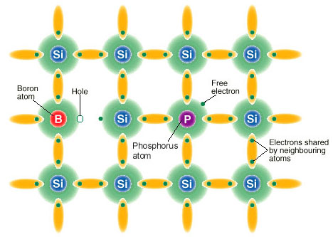
An exaggerated view
of a semiconductor lattice containing
a boron and a phosphorus dopant.5
Now that we know how
semiconductors work, lets discuss how we can assemble them into devices
capable of converting sunlight into electricity.
Web Project
by P. D. Wallace
University of Alaska Fairbanks
|


