A combination of voltage sources, grounding points, and input/output pins are used to implement electronic logic gates. Rather than explain in excruciating detail up front, it may be best to first see a very simple logic gate implementation.
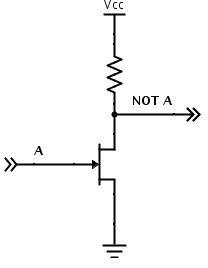
This gate has one voltage source at the top (\(V_{cc}\) and \(V_{dd}\) may be used interchangeably), one ground at the bottom, one input on the left (A), and one output on the right (NOT A). The resistor in the gate is used to lower the current flowing through the circuit. The diagram element at the junction of the input, output, and ground is a transistor. Transistors can act as electronic switches - they control whether or not a circuit path is opened or closed based on whether their input line is high or low. This transistor lets current flow to ground when it is activated by a high input, and breaks its portion of the circuit when it is deactivated by a low input. This break forces current to flow through the output pin. In this manner, the output is the inverted input - high when the input is low, and low when the input is high.
The transistor in the diagram is an NMOS transistor, meaning that it is a MOSFET (metal-oxide-semiconductor field effect transistor) whose natural state is open. When its input is active, an NMOS transistor is "pulled down" into a position that allows current to flow across its bridge, leading to the name "pull-down network" for the collection of transistors that perform logic in an NMOS-implemented gate.
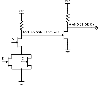
The basic operators in boolean algebra (NOT, AND, OR) do not transfer nicely over into transistor logic. It should be fairly easy to see how the functionality of an AND gate is implemented with transistors in series, and how OR functionality may be constructed using transistors in parallel. The problem is that when the transistor inputs match a '1' condition on the appropriate truth table, current flows to ground. This makes NMOS transistor logic naturally inverting. The transistor-based implementation of AND yields NAND, and OR's natural implementation yields NOR. NOT is already an inverting gate, so its implementation is as shown above. To get the appropriate basic operator, a NOT must follow any naturally-inverting function. Here is an NMOS implementation, complete with trailing inverter, of the boolean function \(a(b + c)\):

