| Quick Links Title | Introduction | Electromagnetic Radiation | Photons Traveling to Earth | Photoelectric Effect | Sources |
| Photoelectric Effect The photoelectric effect is a material's ability to create an electric voltage or current upon light exposure. PV cells have to be material with the photoelectric effect. When In the previous page the amount of electrical power potential was explored; this page looks at a much smaller scale where the electromagnetic particles are interacting with objects of relatively small surface area. Photovoltaic cells are made of semiconductor material that has been treated in order to create an electric field that has a positive and negative that applies to circuit terminals. The cell is composed of a selection of materials in order to create a P-N junction, which acts as a diode. Photon Interaction with Semiconductors Semiconductor material has a characteristic called the band gap. The band gap is a measure of energy in electron-volts (eV) or Joules. If a photon comes into contact with a semiconductor the energy level of the photon and the band gap of the semiconductor will determine what will happen next. When a photon has a lower energy than the semiconductor's band gap it passes through the semiconductor with little effect. For the semiconductor to produce a charge the photon that strikes it must have an energy level equal to or greater than the semiconductor's band gap. Common semiconductor band gaps are readily available and the energy level of the photons can be determined through physics and math.  The above equation will tell
determine how a photon interacts with a
semiconductor with a given band gap. In the
equation h is Planck's constant, c is the speed of
light, and
 wikipedia.org 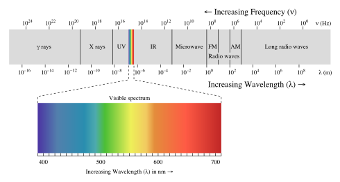 wikipedia.org Typical semiconductors are made with silicon and then the cell is dope to make a P-N junction that acts as a diode. The diode characteristic enables the cell to have current flow in the direction from the positive to negative, but not the other way around. This effect of doping to make a P-N junction can be explained with physics. The basic concept behind doping is to add elements to the silicon in order to give it a generally positive or generally negative potential. Silicon has 4 valence electrons and when it bonds it creates a tetrahedral crystal. If material from group III is added, such as boron, then the 3 valence electrons from boron bond, but there is a missing bond which leaves a "hole." The "hole" that is created with boron doping acts as a positive charge because it attracts the negative charge. Doping silicon with boron gives p-type material. When silicon is doped with an element from group V, such as phosphorus, then 4 of the valence electrons of phosphorus bond, but there is one valence electron left that has the higher ability to flow. Doping silicon with phosphorus makes n-type material. When the n-type and p-type material are then placed in contact some of the available "holes" in the p-type material move to meet with some of the available electrons; this bond forms the barrier which limits flow. Before the barrier cuts off the flow of current, the n-type material lost electrons through attraction to the holes and gives the n-type material a quantitative positive charge as it lost electrons and this creates an electric field. Because there is separation between the two materials there is a potential for current flow that will not be achieved until a circuit is completed to both sides. 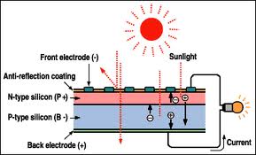 www.wcubed.com Current Flow for
Electrical Power Applications
As photons strike the semiconductor electrons are knocked free and given the ability to flow. If the energy determined by the wavelength is less than the band gap there will be no change in the electron state or charge. When the energy of the photon exceeds the band gap it will knock free the electron and then continue to interact with the semiconductor dissipating its energy through small transfers and heat loss. So as photons are "pushing" the electrons to flow, there has to be a system in place in order to harness it. On the sides of the cells there are conductive metal plates that store the electrons and when a circuit is built from the positive to negative terminals, the electron flow will effect the components of the circuit. Typically there will be the cell with conductive plates and wires going to a charge controller and battery. PV cells produce direct current so the battery will become charged and available for use as electricity. DC to AC converter are common components after the battery which will then run to outlets or devices requiring AC.  |