What is it?
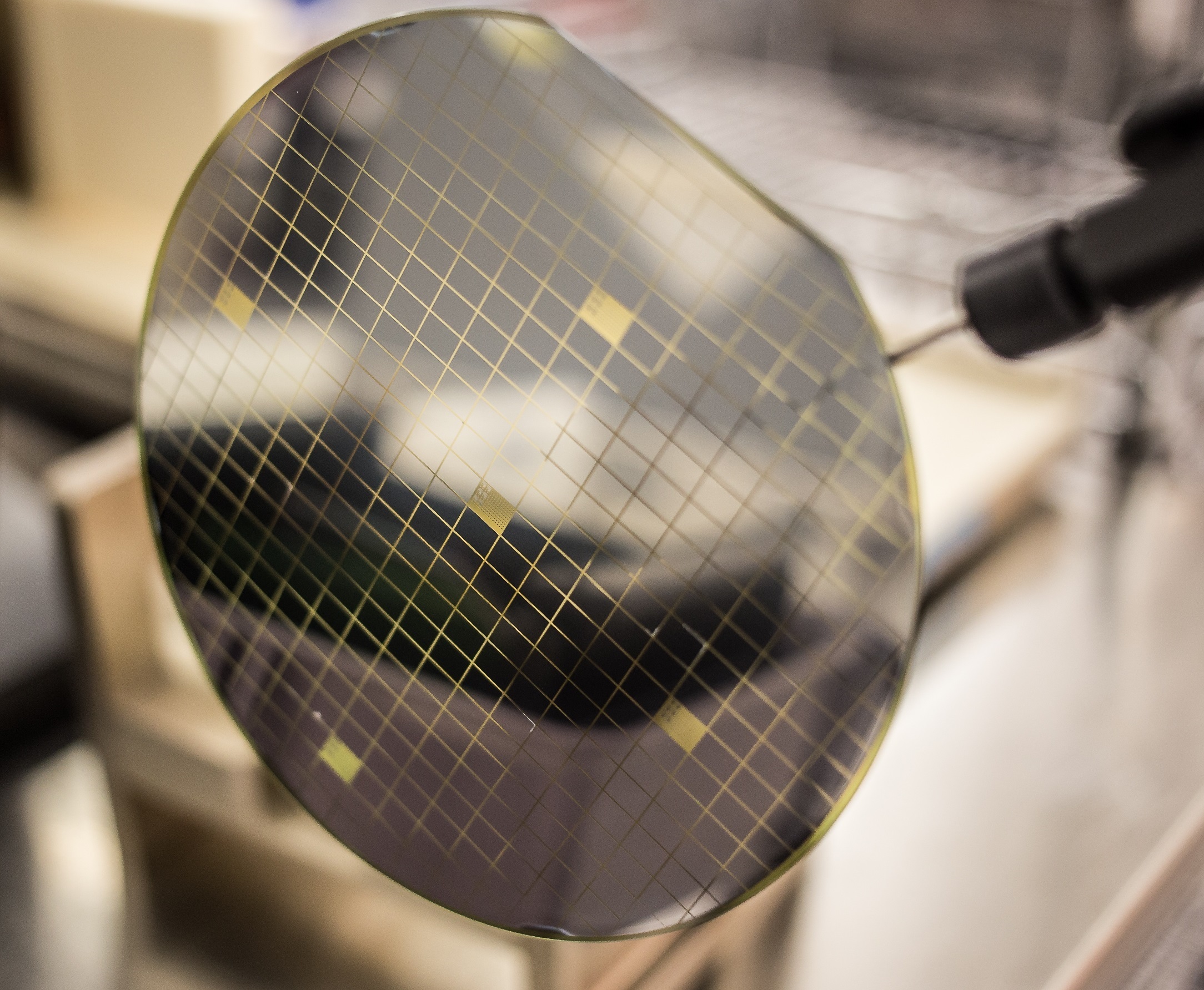
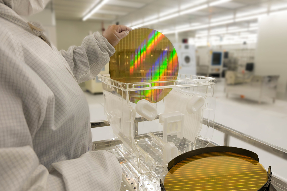
Photolithography is the process used to apply patterns onto a silicon wafer. This process is typically repeated several times, until multiple layers (20+) are created. These layers can consist of different materials, and all of them are interconnected (wired) very specifically. All of them can also be doped.

This process is done in order to make silicon wafers useful in computing, since they don't provide any function by themselves. Silicon is a renowned semiconductor, chosen for its ability to conduct or not conduct current, which is a useful property for producing electronic circuits. This property is useful because computers operate in binary at the lowest level; in 0s and 1s. Those 0s and 1s are simulated physically by semiconductors, like silicon, by alternating between conducting and not conducting current.
Photolithography is an especially important factor in improving the performance, energy efficiency, and density aspects of semiconductors. This is because the size of lasers used during this process determine the size and form of the structures formed out of silicon wafers. These structures such as transistors, resistors, diodes, and capacitors.
The size of the lasers used for forming these structures is a characteristic of what's known as a "process node". These process nodes are named accordingly to their primary characteristics (e.g. laser size), so as to help differentiate different lithography processes from each other. There are several semiconductor fabrication firms around the world that develop at their own pace and with their own characterstics from one process node to another, so being able to differentiate them all by names and specifications is crucial.
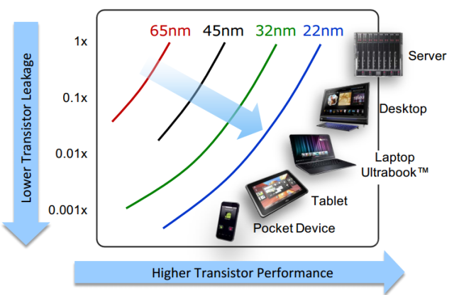
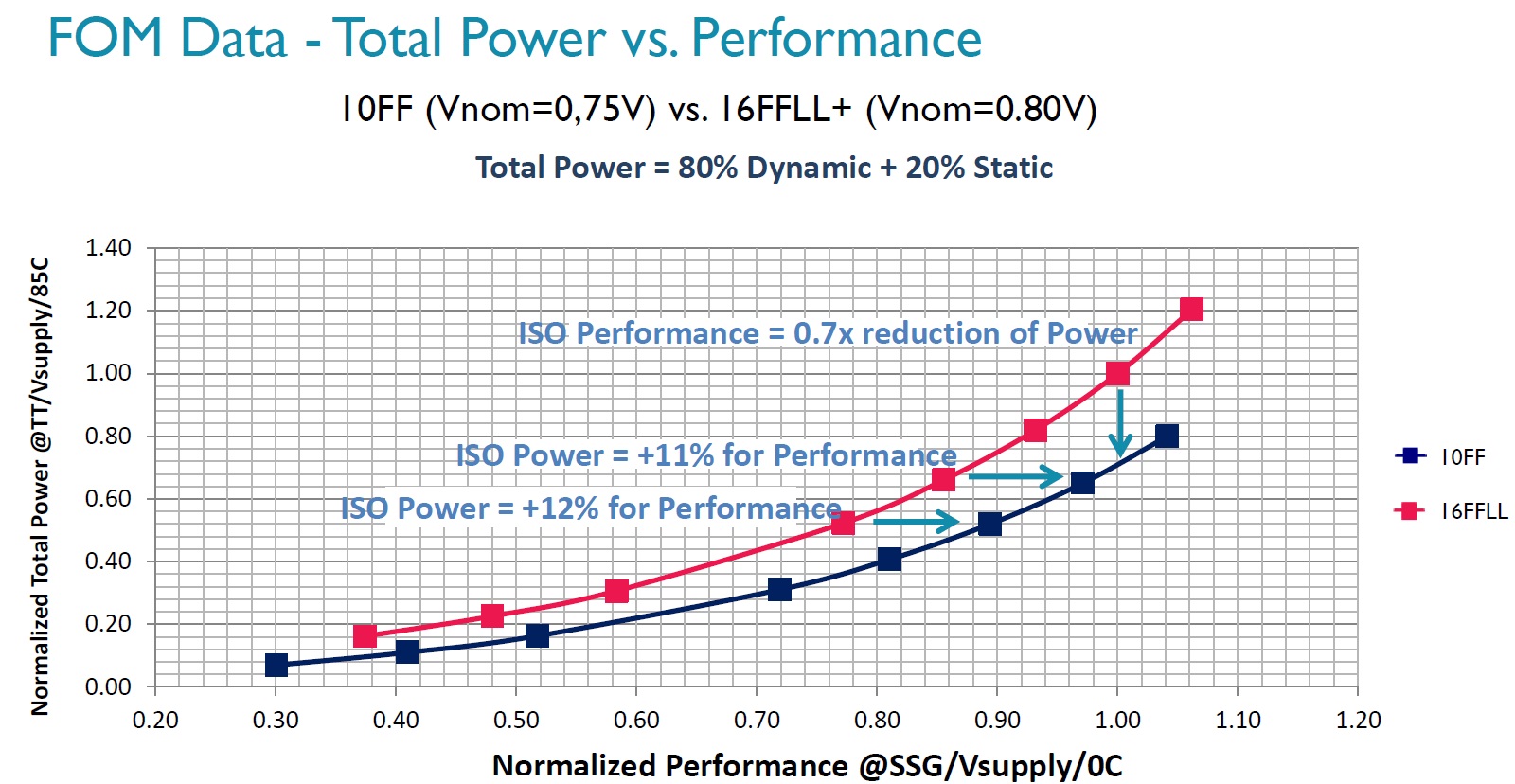
As process nodes have improved since the inception of integrated circuit processors, the size of their components (mostly transistors) have shrunk from thousands and hundreds of nanometers to only several tens of nanometers today. This means there is greater density of these individual components in these ICs, as well as improved performance and/or energy usage. It's important to note that only 2 of these 3 improvements can be maximised at once, so engineers have to decide what characteristics they wish to improve with each successive process node.
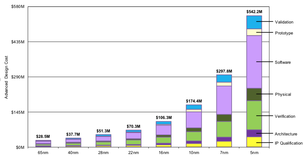
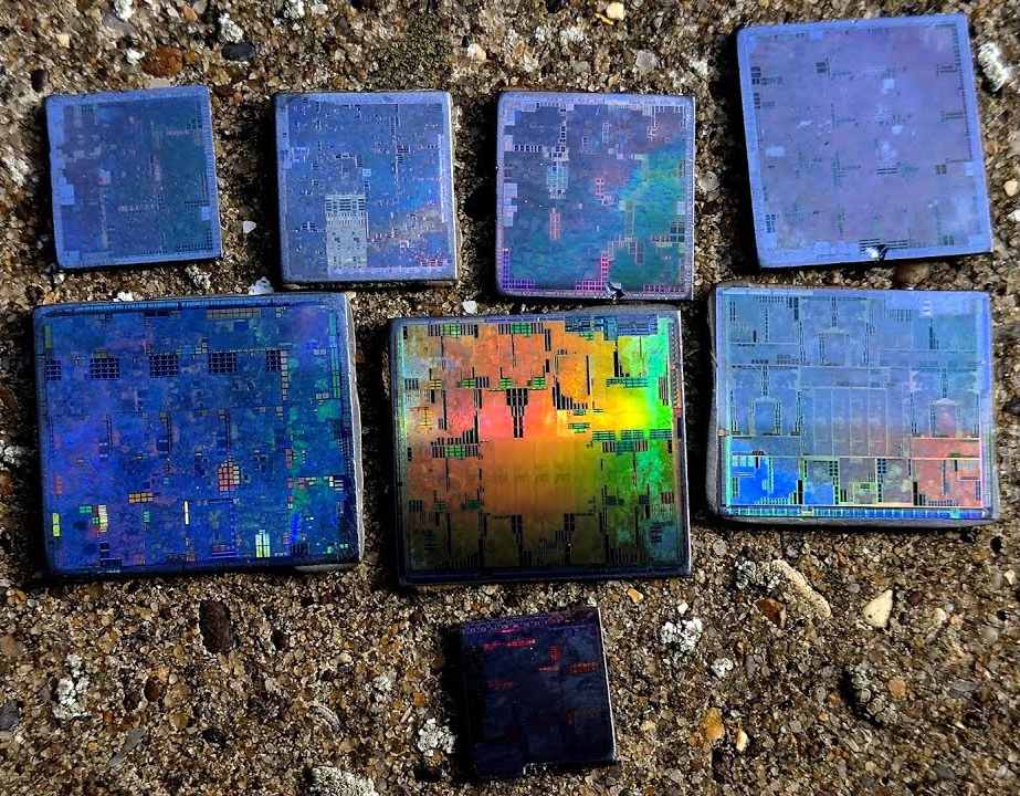
One other significant aspect of photolithography is the economics of the process. It's not an inexpensive process to carry out, let alone carry out well; consequently, there are only a handful of major semiconductor fabrication firms around the world. Each of these "fabs" has to maintain good financial standing in order to not collapse under debt. The economics of each process node is heavily determine by the yields of each silicon wafer. This is simply how many fabricated ICs on a wafer perform as intended out of the total number of ICs physically on the wafer. This is usually expressed as a percentage (e.g. 90% yields for a 14nm process node). Additionally, the way the photolithography process is carried out, there are more functional ICs towards the center of a wafer than around the edges of the wafer, so this is always accounted for before a wafer is processed.
How is it done?
There are multiple steps in order to get to the final, usable silicon wafer product.
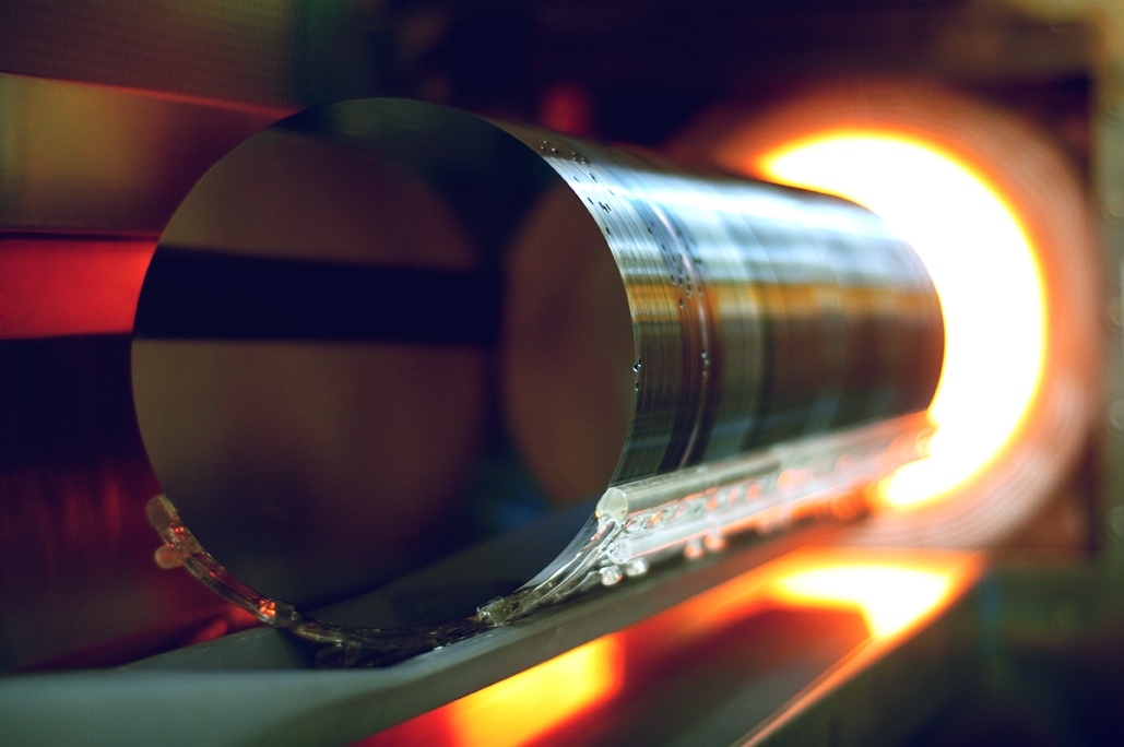
- To begin, the wafer needs to be chemically cleaned. Any impurities, organic, ionic or metallic, can affect the wafer negatively or affect the adhesion of the patterns.
-
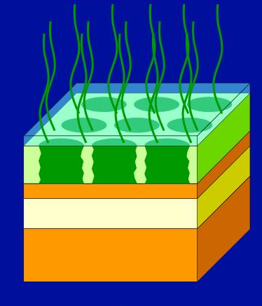
After the intensive cleaning, silicon dioxide is applied to the surface of the wafer to create a barrier layer where the photoresist will be applied.
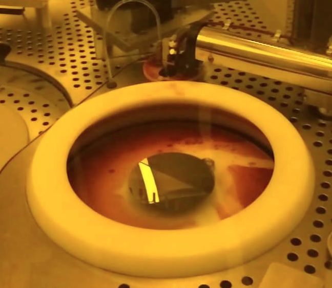
The photoresist layer is applied by a spin coating method in order to be evenly thick throughout the entire wafer surface.
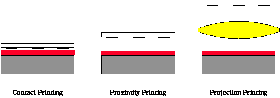
Note that there are two types of photoresist: positive or negative. Depending on the purpose of the silicon wafer, one or the other is used.
With positive photoresist, the mask contains an exact copy of the pattern which is to remain on the wafer and negative resists behaves exactly opposite of this. The negative resist will contain an inverse of the patter to be transferred.
-
After the photoresist is applied, a soft baking process takes place.
This step is to remove all the solvents from the photoresist coating. The soft-baking process makes the photoresist layers become photosensitive or, in other words, susceptible to photo-imaging. The resist is dried in this step and adhesion is improved.
-
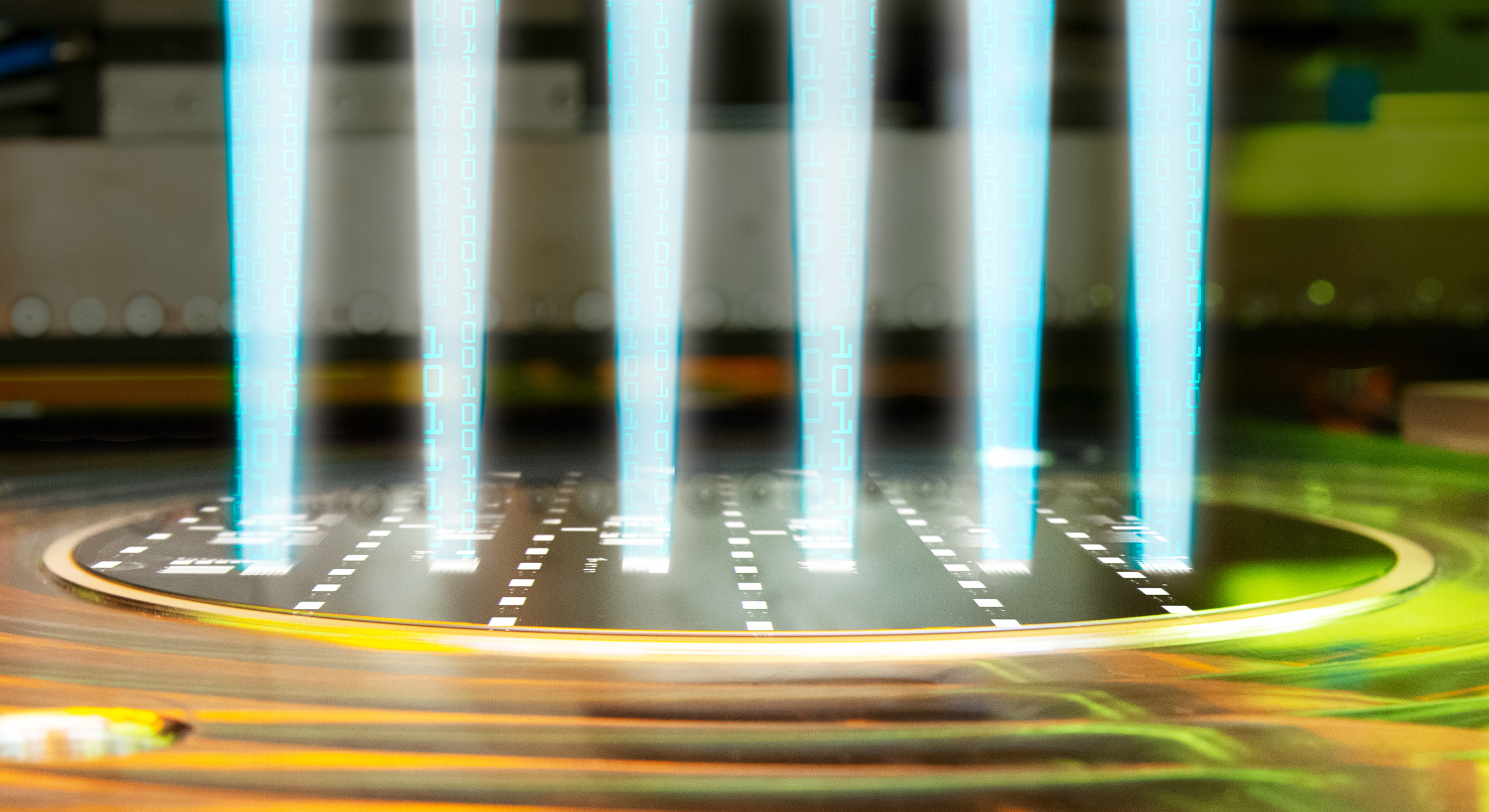
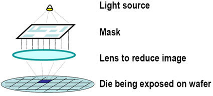
The next step is mask alignment and exposure. The pattern that needs to be transferred onto the wafer is at this point aligned with the wafer.
Each mask must be aligned correctly with the previous pattern. Once the mask has been properly aligned, the photoresist is exposed through the pattern with a high intensity UV light.
There are different exposure techniques: contact, proximity and projection printing. With contact, the resist is brought into physical contact with the glass photomask. In proximity printing, there is a small distance maintained during exposure and with projection there is a larger distance maintained. Projection printing is the most common method of exposure used today because of the mask damage that can occur with the first two methods.
-
Now the post exposure bake and development phases begin, where first the standing waves are reduced and then the shape of the photoresist profile and line width control are determined.
In these phases, the photoresist is stabilized and hardened. These steps are also important in improving the adhesion of the photoresist to the wafer surface. The patterns at this point have been transferred and then the photoresist must be stripped after the imaged wafer has been processed.

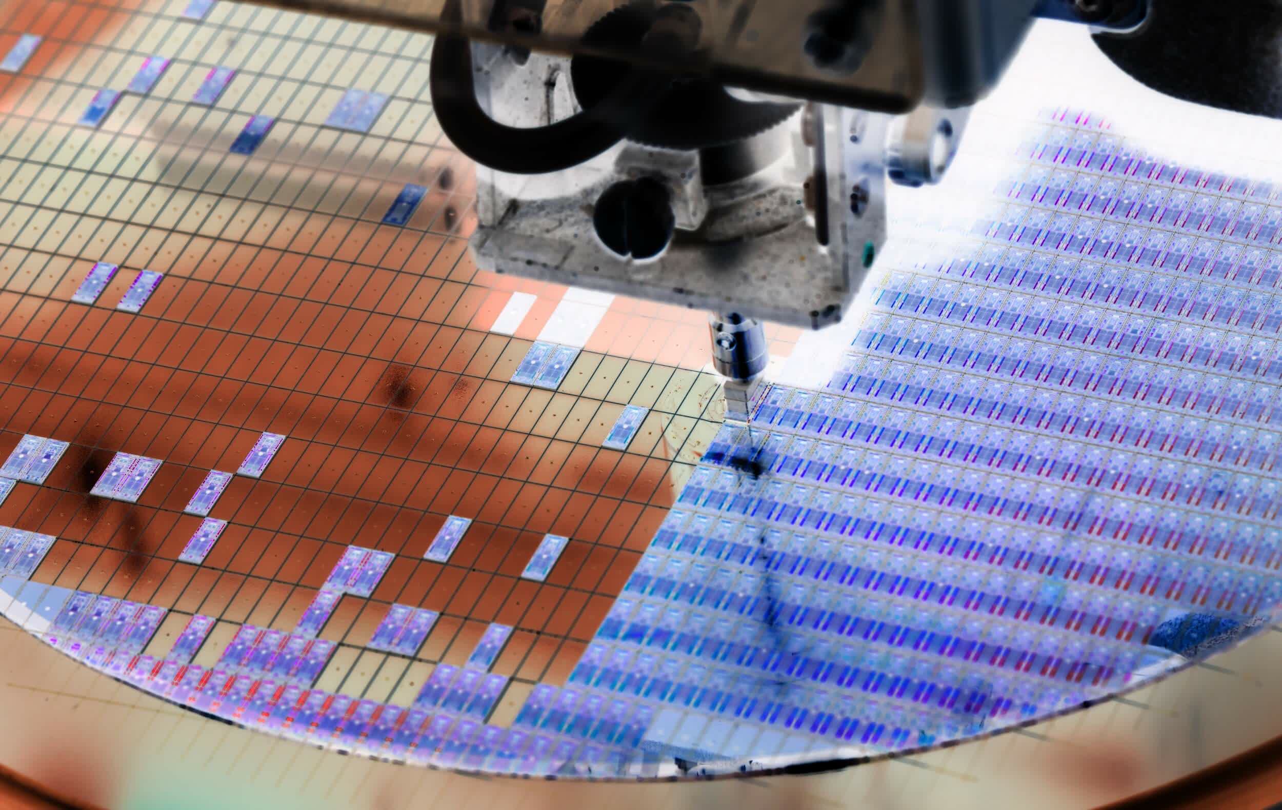
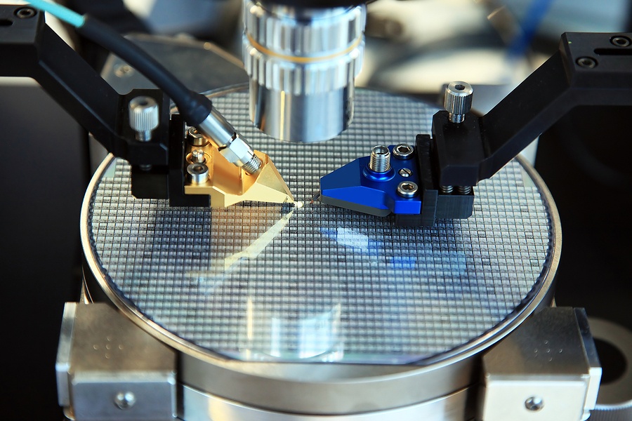
- The laser engraving process is where the perfectly smooth surface of silicon wafers is formed into all the channels and structures that a processor would use to direct and control electrical current. This is the end of the photolithography process, and the silicon wafer is ready to be further processed for its next destination.
Applications
Photolithography is what makes many modern electronics possible, so it is naturally found in numerous applications, such as:
Semiconductors/Computing
- Integrated Circuits (ICs)
- Processors
- Diodes
- Transistors
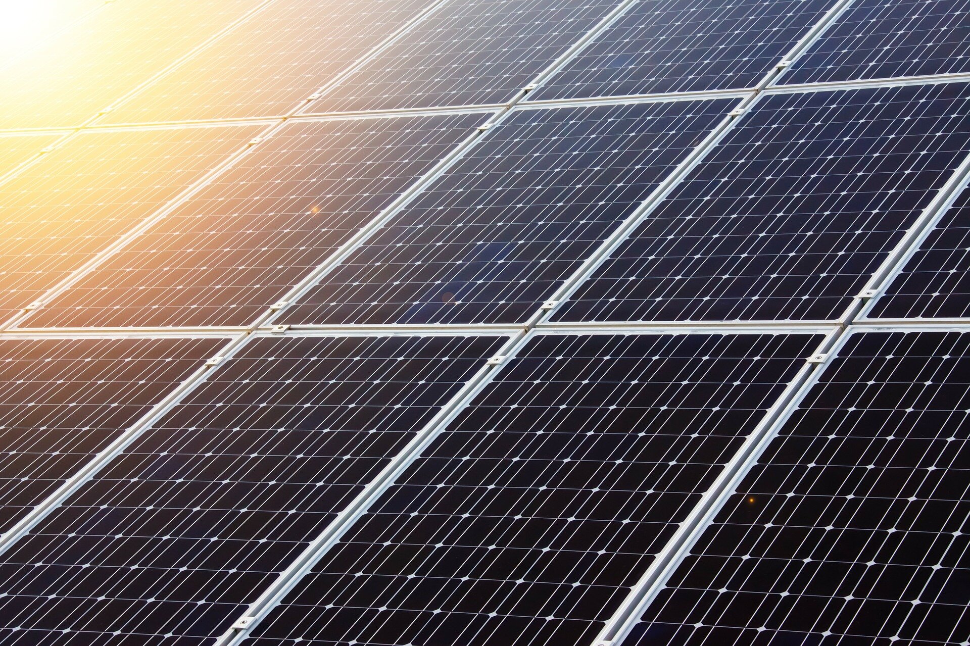
Solar Cells
- Solar-Powered Calculators
- Satellite Power
- General Solar Panels

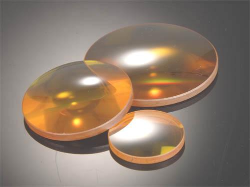
Optics
- IR and Reflective Optics
- Fiber Optics
- Micro-Optic Devices
Conclusion
Photolithography is an important driving force behind many aspects of modern life. Without it, fundamental inventions such as integrated circuits wouldn't exist as they do currently. Photolithography forms blank wafers of silicon into modern marvels, giving them immense function that society has grown to rely upon. Although photolithography might be running into obstacles as semiconductors demand ever smaller sizes of transistors, diodes, resistors, capacitors, and other components crucial for computing applications, this isn't the death knell of photolithography. It's only an obstacle for scientists and engineers to work around as innovation moves along with the help of photolithography.