Basic Transistor Physics
David Giessel
University of Alaska Fairbanks
Physics 212 Web Project, Spring 2003
David Giessel
University of Alaska Fairbanks
Physics 212 Web Project, Spring 2003
| Index | Transistor Basics | Temperature vs Frequency | Gate and Wiring size | Transistor Count | Bibliography | |
Gate and Wiring size
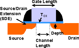
Transistor Gate
The size of transistors on a modern microprocessor is of critical importance to its ability to operate at acceptable frequencies. Modern processors have gone beyond limits thought to be unreachable only a few years ago. Wiring sizes are as small as .09µ (90 nanometers...90x10^-9m!!). That is TINY. And .06µ processes are being developed currently. This reduction in gate size along with smaller wiring diameter translates to lower voltage levels for discrete (off and on) operation. This translates to lower current...which GREATLY reduces I^2R losses (P=I^2 * R). One thing to note is that resistance actually goes up as components shrink as wire diameter is smaller...but because the current is squared in the power calculation, this increase in resistance is small compared to the decrease in current when related to overall power consumption.
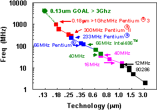
Gate Size vs Frequency
Another important development in lowering current requirements is copper wiring (older CPUs use Aluminum for the wiring). IBM developed copper wiring technology back in 1997. This technology was implemented in the consumer market in the form of the G3 (or PowerPC 750) CPU used in many Macintosh computers starting in '98 to this day. The G3 has gone through several iterations since it was first introduced but thanks to copper wiring even the oldest G3s had power consumption numbers in the range of 5 watts. This is compared to the Pentium II (the x86 CPU of choice at the time of the G3s introduction) at the time consuming 20 watts or more at a similar clock. AMD and Intel were about 2 years behind IBM in implementing copper wiring. The K7 core was AMD's first core to use copper wiring (Thunderbird core to be exact). Intel was the last company to move to copper wiring on its CPUs (they only made the move in the last year or two).
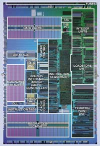
IBM G3 Die Overlay
Other technologies developed to lower I^2 * R losses include SOI (silicon on insulator). This technology (first implemented by IBM) applies a thin layer of silicon to the chip wiring and gate in order to reduce capacitance which therefore reduces the time constant for the circuit...which translates to higher frequency operation. IBM was also the first to implement Low K Dielectric insulation for wiring (called SiLK). This process involves coating the wiring with an insulative compound to increase insulation between wires. This reduces leakage current and interference between signal traces.
Gates are becoming increasingly efficient thanks to these advancements, which leaves only one area to further reduce power usage: lowering the number of transistors.